
Cleaning Solutions
From Solvents to Plasma: The Green Surface Cleaning Trend in the Electronics Manufacturing Industry
1. Challenges of Traditional Cleaning Methods
Historically, cleaning PCBs involved organic solvents such as IPA, acetone, or fluorinated chemicals. While effective for removing flux residues, these chemicals present significant drawbacks.
- Emission of VOCs (Volatile Organic Compounds) causing air pollution
- Health risks for production operators
- High wastewater treatment and disposal costs
- Difficulty meeting modern environmental standards such as RoHS and REACH
As governments and global supply chains demand greener processes, traditional solvent cleaning is becoming less sustainable and more expensive to maintain.
2. Transition to Solvent-Free Cleaning Technologies
To address these challenges, manufacturers are increasingly adopting advanced dry cleaning technologies that eliminate the need for liquid solvents.
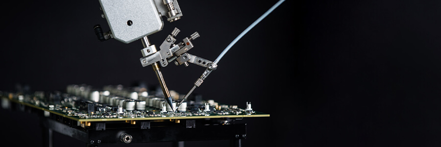
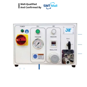
- CO₂ Snow Cleaning: High-pressure solid CO₂ particles remove contaminants without leaving residues.
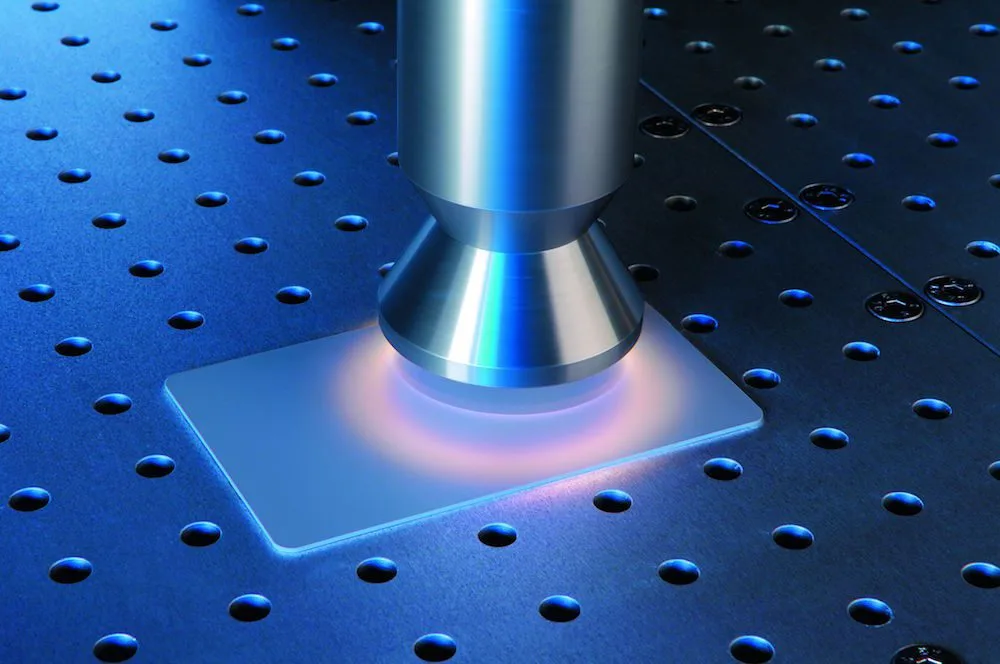
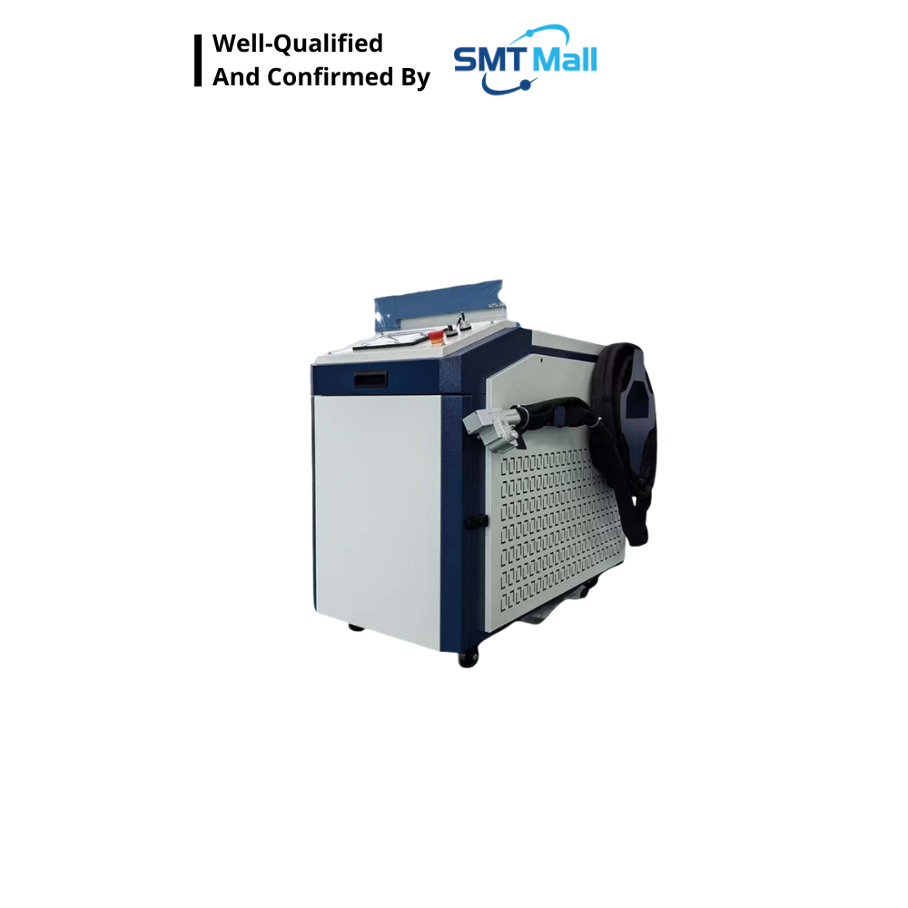
- Laser Cleaning: Laser pulses vaporize oxides and contamination with extremely high precision.
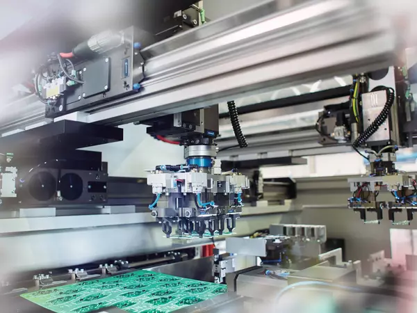
- Plasma Surface Cleaning: Ionized gas removes organic residues while activating the surface.

3. Why Plasma Leads the Green Cleaning Trend
Among modern cleaning technologies, plasma surface treatment has become one of the most promising solutions for sustainable manufacturing.
- No chemical solvents: Only process gases such as O₂, N₂, or Ar are used.
- No liquid waste or VOC emissions: Reducing environmental impact.
- Energy-efficient operation: Short processing time and low power consumption.
- Improved product quality: Surface activation enhances adhesion for solder, coating, or bonding.
These advantages allow plasma technology to meet RoHS and REACH compliance requirements while supporting ESG and sustainability goals.
4. The Future of Green Electronics Manufacturing
The shift toward green cleaning is no longer optional — it is becoming a mandatory standard for manufacturers seeking to participate in global electronics supply chains.
By adopting solvent-free technologies such as plasma cleaning, companies can reduce operational costs, improve environmental compliance, and move toward smarter, more sustainable production systems.
Investing in modern cleaning technologies like plasma not only improves PCB reliability but also aligns your production line with the future of green and intelligent manufacturing.
Discover Green Cleaning Solutions →
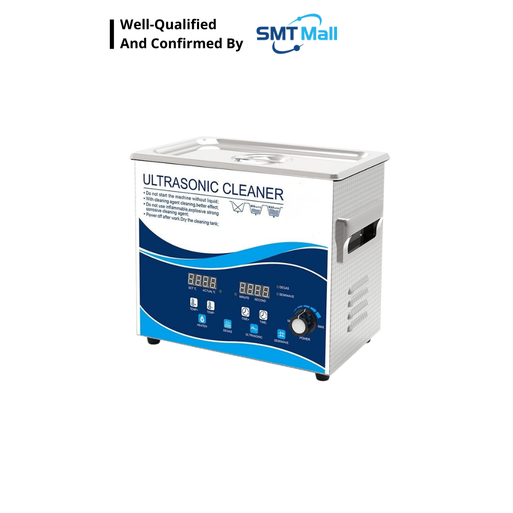
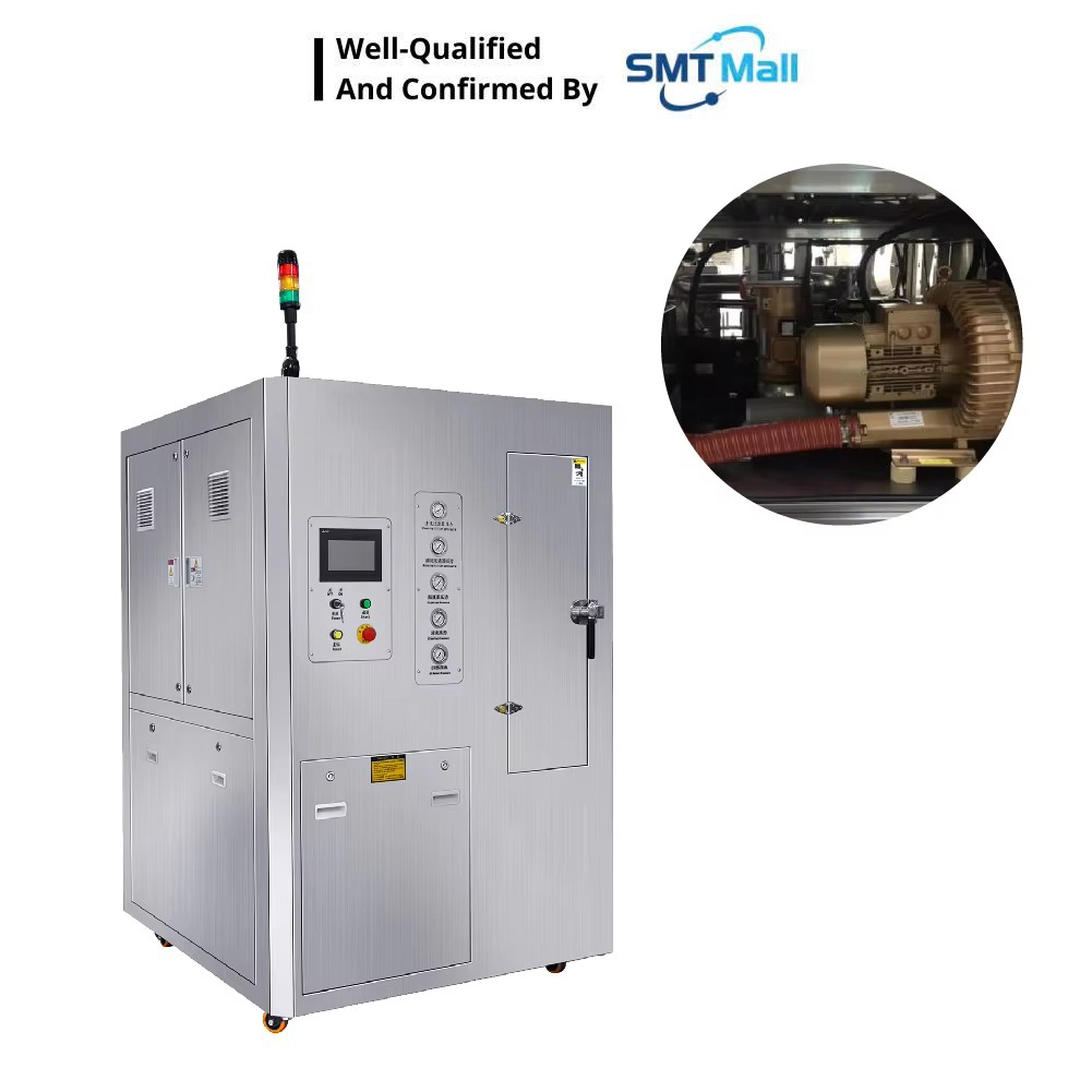
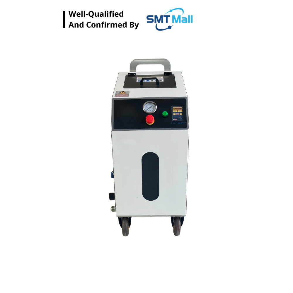
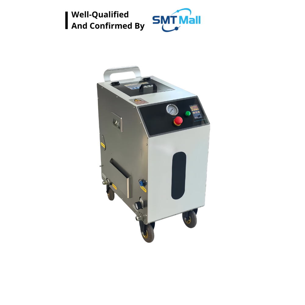
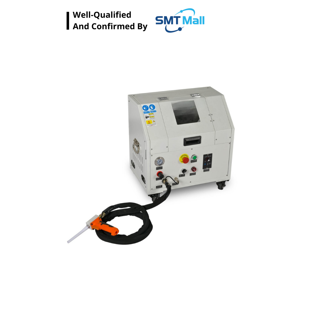
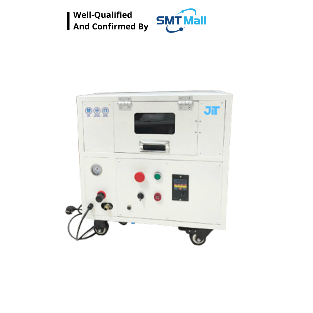
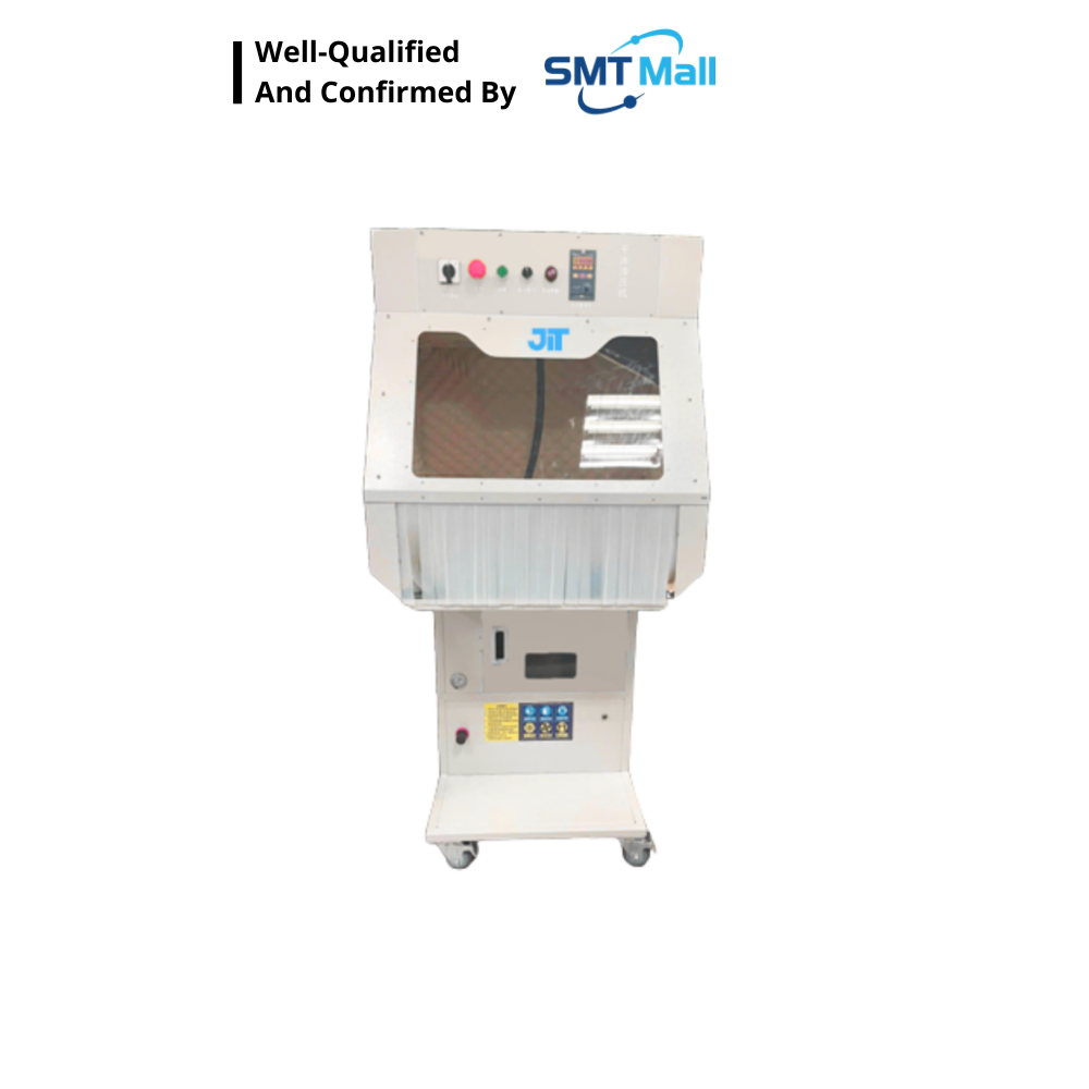
Recommended PCB Cleaning Machines
We offer a variety of PCB cleaning machines ideal for your cleaning application.
$ 35,000.00
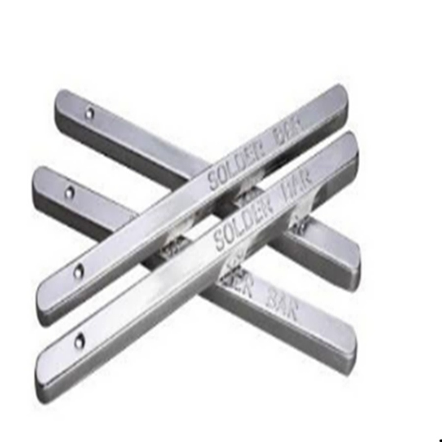
Cleaning solutions
$ 79.00
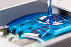
Cleaning solutions
$ 51,816.87
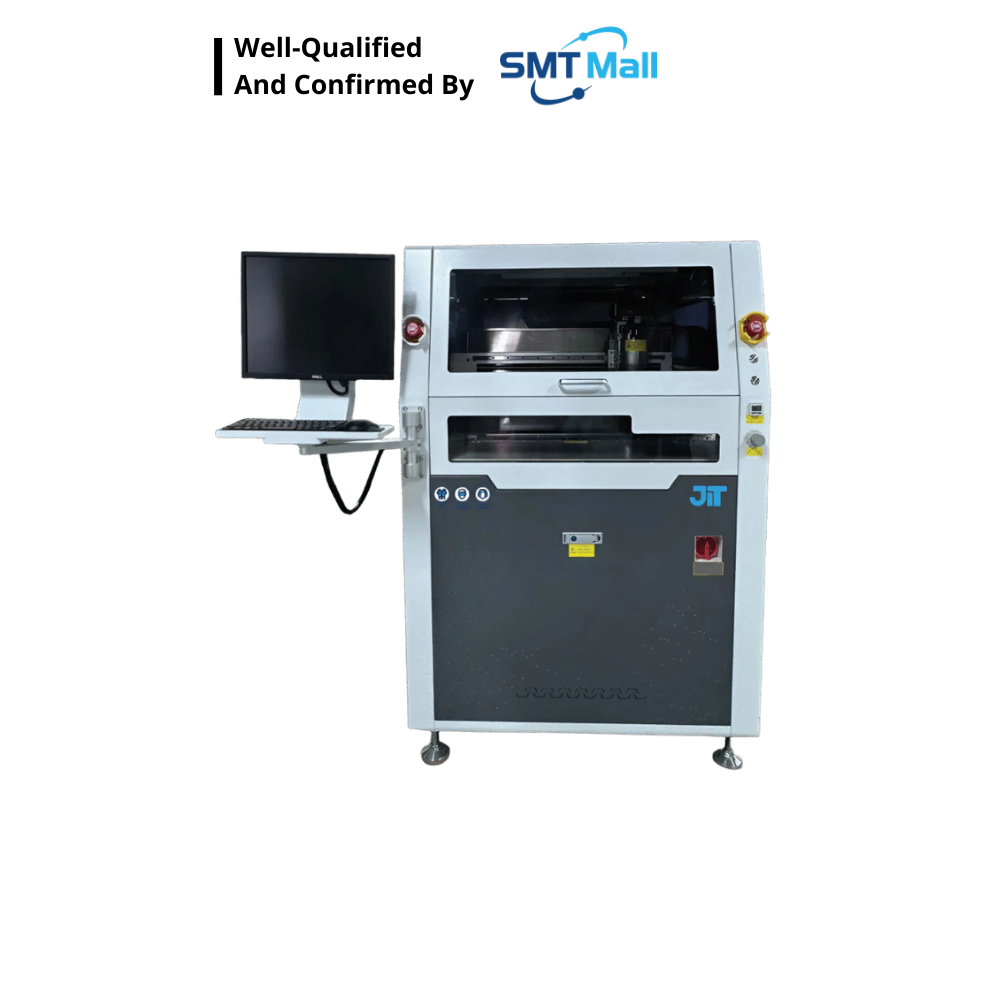
Cleaning solutions
$ 4,200.00
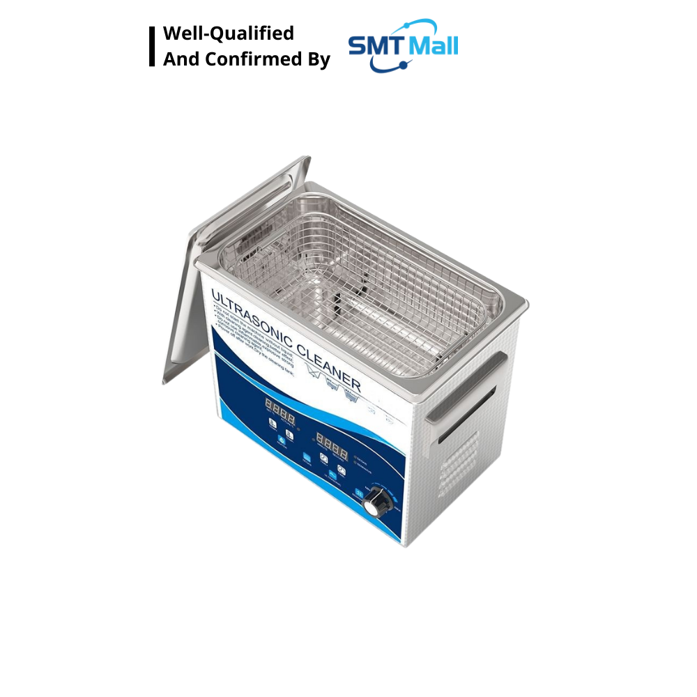
Cleaning solutions
$ 1,920.00
Cleaning solutions
$ 2,150.00
Cleaning solutions
$ 3,220.00
Cleaning solutions
$ 27,300.00