
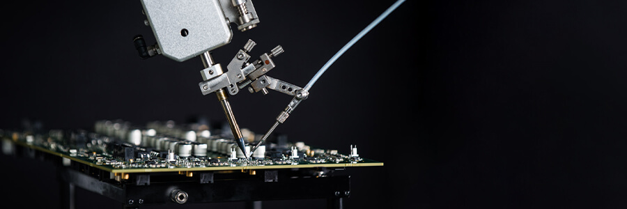

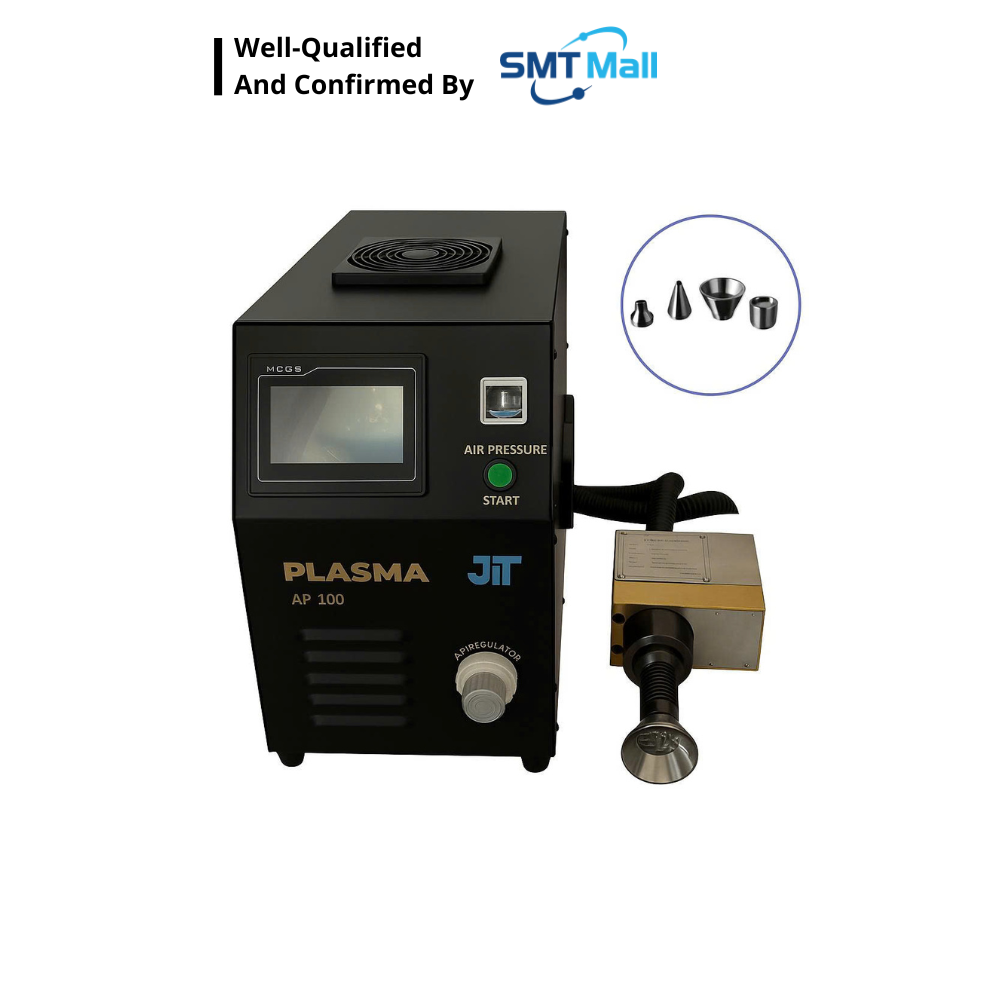
Surface treatment solution
Plasma Surface Treatment Process in Electronic Component Manufacturing
1. What is Plasma Surface Treatment?
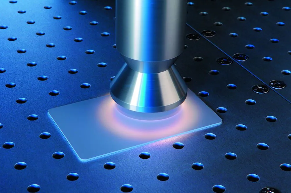
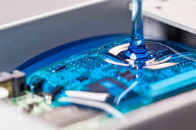
Plasma surface treatment utilizes plasma — a highly energized state of matter composed of charged ions, electrons, and reactive species — to modify material surfaces. In this environment, high-energy particles break chemical bonds of contamination layers, effectively removing oil, dust, oxides, and organic residues.
As a result, the material’s surface energy increases dramatically, improving wettability and enhancing adhesion for adhesives, coatings, conformal layers, and solder materials.
2. Working Principle
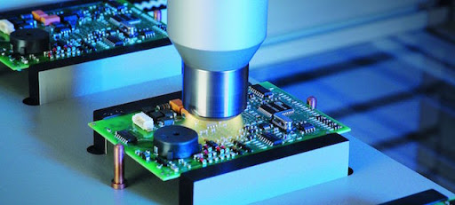
Plasma systems typically generate ionized gas under controlled low-pressure conditions. When plasma interacts with a surface, active species such as O•, N• radicals, or Ar⁺ ions:
- Decompose surface contaminants and organic residues
- Remove thin oxide layers
- Introduce polar functional groups (–OH, –COOH)
- Increase surface wettability and bonding capability
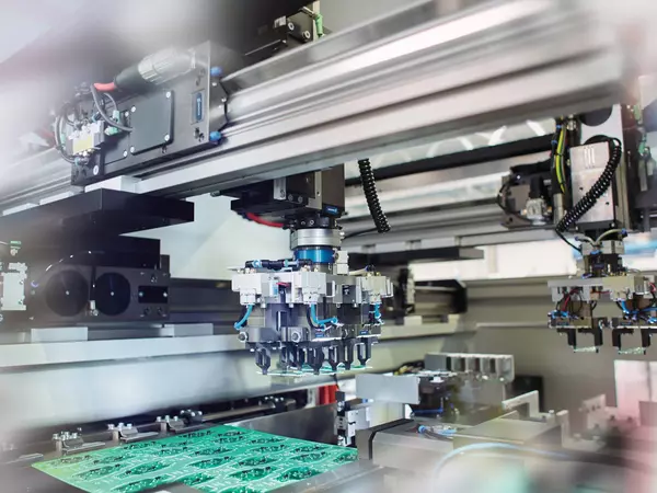
3. Plasma Surface Treatment Process Flow
- Step 1 – Material Preparation: Pre-clean PCB, plastics, or metals to remove visible dust and oil.
- Step 2 – Plasma Setup: Select process gas (O₂, N₂, Ar) and configure power, pressure, and time parameters.
- Step 3 – Surface Activation: Ion bombardment removes contamination and forms active functional groups.
- Step 4 – Inspection: Verify surface energy using Contact Angle Test or Surface Energy Measurement.
4. Future Outlook in Smart Manufacturing
As industries shift toward environmentally friendly production, plasma treatment stands out for its solvent-free operation, low energy consumption, and high process consistency.
In the coming years, plasma technology will play an increasingly important role in semiconductor packaging, automotive electronics, renewable energy modules, and advanced PCB assembly lines — driving higher product quality and sustainable manufacturing.
Plasma surface treatment is not just a cleaning method — it is a precision activation technology that enhances adhesion, improves reliability, and supports the transition toward green, intelligent electronics manufacturing.
Explore Plasma Treatment Solutions →Recommend Treatment Solution
$ 35,000.00
$ 5,000.00